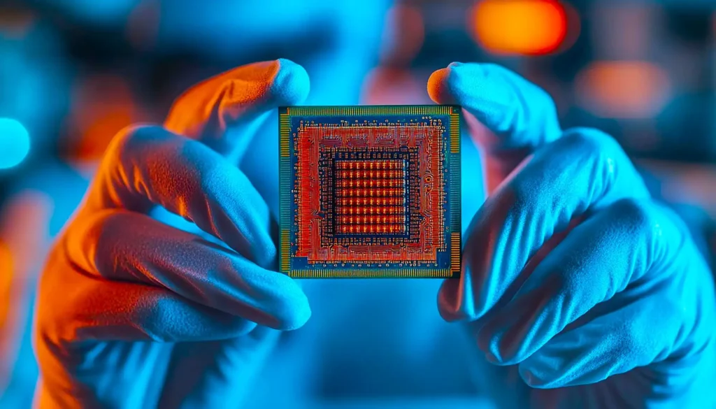
Real-world tapeout is a pivotal milestone in the journey from digital schematics to mass-produced semiconductor chips. For aspiring chip designers, understanding tapeout is not just a technical necessity; it’s a foundational experience that shapes their perspective on the entire VLSI (Very Large Scale Integration) design flow and reveals the tangible impact of their work in a high-stakes, real-world context.
At its core, tapeout marks the transition from design to manufacturing. Historically, the term originated from the era when design data was stored and transferred on magnetic tape, but today, it still refers to the point when the final chip design is submitted to a semiconductor foundry to fabricate the physical device. This submission includes a complete and rigorously checked digital description of the chip’s geometry, which is then used to create expensive photomasks for the lithography process. After this, any changes become exceptionally costly and time-consuming, highlighting why the tapeout is treated with utmost seriousness by professionals and companies alike.
Why is tapeout so crucial for aspiring designers?
- It forces designers to confront the difference between simulated and real-world results. Even perfectly simulated chips can display new issues during physical fabrication, such as unexpected electrical interactions, manufacturability flaws, or layout rule violations. Exposure to this process teaches respect for the physical constraints and real-life challenges of chip production.
- The cost and risk at tapeout are immense. A mistake at this stage can require re-spins, design revisions that often incur millions of dollars and delay market entry. Therefore, aspiring designers quickly learn the value of meticulous checking, collaborative reviews, and rigorous testbench creation.
- Tapeout isn’t just about design. It involves tight coordination between multiple teams such as verification, physical design, validation, and foundry interface engineers. Being part of a real-world tapeout is an education in clear documentation, version control, status tracking, and cross-functional collaboration.
- Successful tapeouts bring new technologies to market, from GPUs to specialized AI accelerators. The tapeout experience links an engineer’s work directly to visible technological advances and commercial success.
- In an industry where time-to-market is critical, familiarity with tapeout deadlines, mask preparation, and manufacturing constraints allows young designers to contribute to projects that won’t just work in theory, but will deliver competitive products under real-world pressures.
For aspiring chip designers, there is no substitute for the lessons learned from participating in real-world tapeouts. It is this crucible that transforms theoretical knowledge into practical wisdom and prepares engineers to deliver reliable, high-performance, and innovative silicon on schedule and at scale.
